abstract.
For this lab, we used L-edit®, a simple program that helps us lay out silicon and metal layers, to draw basic transistors. We first laid out an NMOS transistor and then a PMOS transistor. Then combining these (CMOS) we constructed an inverter gate, a nand gate and a nor gate. We then extracted out layout and simulated our gates in SPICE®. Finally, we created a 4-input nand gate in two ways; first using CMOS to build one from ground up, and second by combining the NAND, NOR and the inverter gates.
task 1 : inverter (NOT)
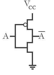
Figure 1. the inverter (not gate)

Figure 2. the inverter layout (click on image for larger version)
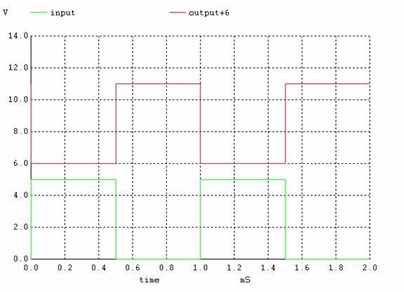
Figure 3. SPICE output for the NOT gate.
SPICE circuit file for the inverter.
| NOT gate |
input |
output |
0 |
1 |
1 |
0 |
Table 1. NOT gate (inverter) output
task 2 : NAND gate
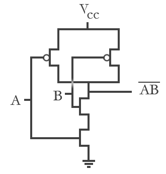
Figure 4. the NAND gate
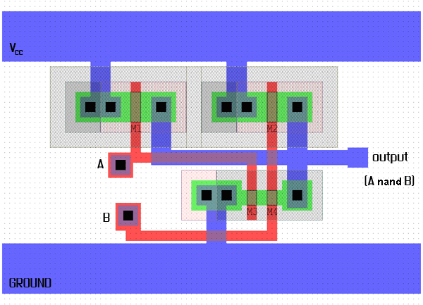
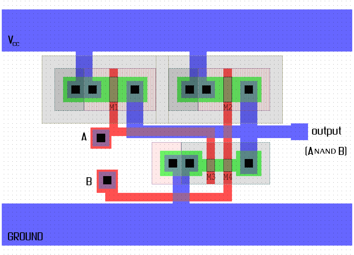
Figure 5. the NAND gate layout (click on image for larger version)
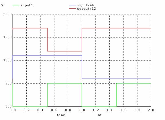
Figure 6. SPICE output for the NAND gate.
SPICE circuit file for the NAND gate.
| NAND gate |
A |
B |
output |
0 |
0 |
1 |
0 |
1 |
1 |
1 |
0 |
1 |
1 |
1 |
0 |
Table 2. NAND gate output
task 3 : NOR gate
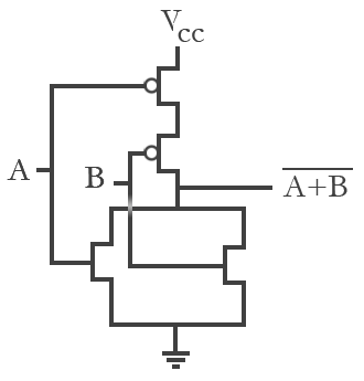
Figure 7. the NOR gate
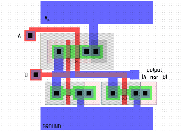
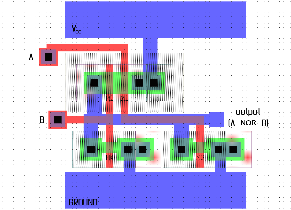
Figure 8. the NOR gate layout (click on image for larger version)
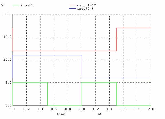
Figure 9. SPICE output for the NOR gate.
SPICE circuit file for the NOR gate.
| NOR gate |
A |
B |
output |
0 |
0 |
1 |
0 |
1 |
0 |
1 |
0 |
0 |
1 |
1 |
0 |
Table 3. NOR gate output
All gates are seen together in Figure 10.
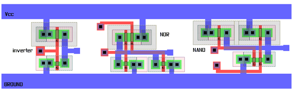
Figure 10. all gates seen together (click on image for larger version)
task 4 : 4-input NAND gate
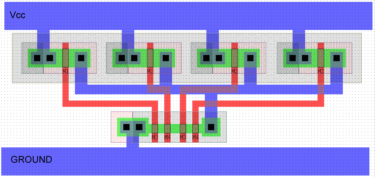
We can create a 4-input NAND gate in two ways. The first way is to layout the circuit in CMOS. Figure 11 shows the layout and Figure 12 shows the layout using L-edit.
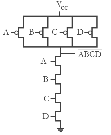
Figure 11. the 4-input NAND gate (CMOS)
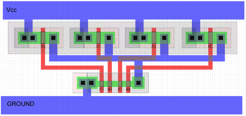
Figure 12. the 4-input NAND gate layout (click on image for larger version)
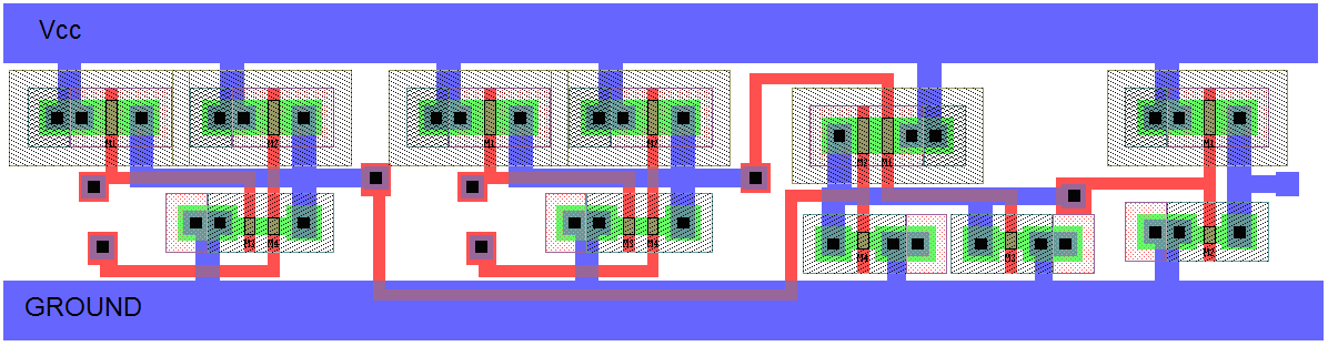
Another way to create a 4-input NAND gate is to use the NAND, NOR and NOT gates we've already created. Figure 13 shows how 2 NAND gates, a NOR gate and a NOT gate can be put together to implement the 4-input NAND gate.
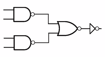
Figure 13. implementation of a 4-input NAND gate using 2 NAND one NOR and a NOT gate.
As an extension, we laid out the gates in L-edit (see Figure 14). A comparison of Figure 14 and Figure 12 shows how much more compact the gate would be if it were built from scratch (and not using other gates).
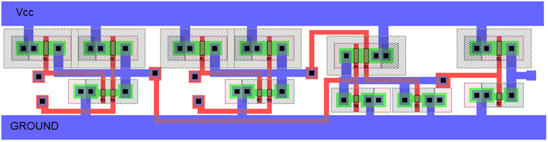
Figure 14. the 4-input NAND gate layout using 2 NAND one NOR and a NOT gate. (click on image for larger version)
|