abstract.
In this lab, we investigated three implementations of an 8-input AND gate and analyzed any differences in the speeds of these three implementations. The number of transistor stages and logic gates differed among the three cases. We used L-Edit to lay out all three configurations and extracted the files for dynamic simulation in SPICE. We discovered that the three configurations have widely different dynamics although each produced the same output logic.
procedure.
We are given a circuit that requires the use of an 8 input AND gate. Shown in circuits A, B, and C in figure 1 are three ways to implement them.
 |
 |
 |
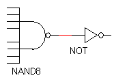
| fig1 a. implementation A |
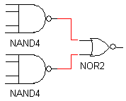
fig1 b. implementation B |
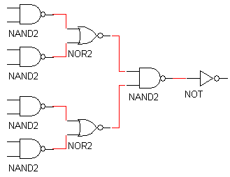
fig1 c. implementation C |
figure 1. three implementations of an 8 input AND gate (these image were taken from the lab procedure)
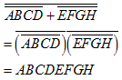
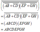
TASK 1 : Verify that the three implementations (A, B, and C) all implement the same logic function (8 input AND)
PART A
PART B
PART C
TASK 2 :
How many transistors are required for each implementation? Which is smallest (# of transistors)?
PART A:
There are 8 transistors in parallel in the pull-up network, 8 transistors in series in the pull-down network of the NAND8 gate and two transistors in the NOT gate. There are a total of 18 transistors.
PART B:
There are 8x2 = 16 transistors in the NAND4 gates and 4 transistors in the NOR2 gate. There are a total of 20 transistors.
PART C:
There are 5x4 = 20 transistors in the NAND2 gates 4x2=8 in the NOR2 gates and 2 in the NOT gate. There are a total of 30 transistors in this configuration.
TASK 3 : Draw a stick-figure diagram for each implementation.
A)
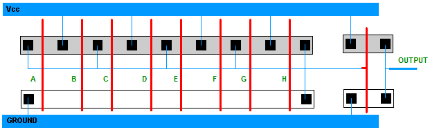
figure 2. Eight input AND gate (version 1) and its stick-figure diagram.
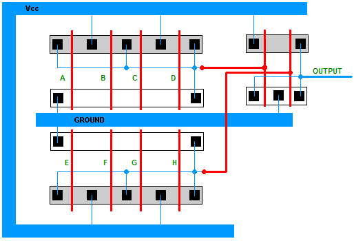
figure 3. Eight input AND gate (version 2) and its stick-figure diagram.
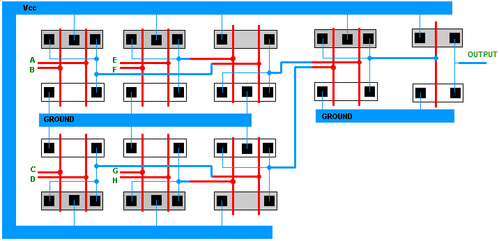
figure 4. Eight input AND gate (version 3) and its stick-figure diagram.
TASK 4: Roughly estimate the speed of the three implementations based on our 2m process transistors. To do this you might first estimate the speed of an invertor, and then use that to estimate the speed of the two, four and eight input gates as we did in class. Clearly state assumptions.
The speed of the three implementations was determined by noting the speed of the invertor and other X-input NAND gates. By selecting a single path from the input to the output, the speeds of the stages were summed for a falling and rising output. The relevant equations are shown below, and simulated in SPICE for an estimation.
 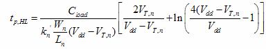 Equation 1 Equation 1
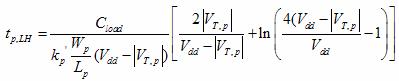 Equation 2 Equation 2
Equations 1 and 2 were taken from Professor Erik Cheever's handout on NAND Dynamics.
1-input NAND (inverter): 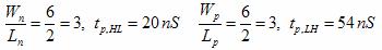
2-input NAND: 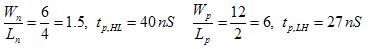
4-input NAND: 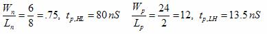
8-input NAND: 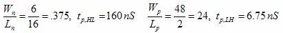
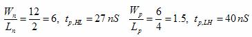
2-input NOR: Assumed equal, but opposite to the 2-input NAND
implementation A: 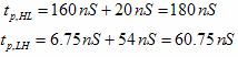
implementation B: 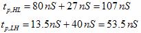
implementation C: 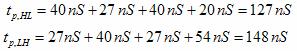
TASK 5:
Write a SPICE deck to simulate each of the 3 implementations when all 8 inputs change
simultaneously. How fast is each implementation? Which is fastest? Is this what you expected? Include the SPICE decks with your writeup.
- Repeat the simulations for the case when all inputs but the highest one are high, and it alone is varying.
- Repeat the simulations for the case when all inputs but the highest one are high, and it alone is varying.
-
Compare the results of the previous two parts.
IMPLEMENTATION A
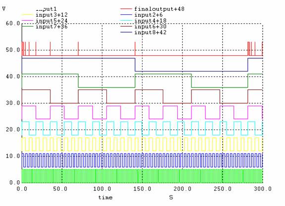
Figure 5. implementation A; all inputs changing simultaneously.
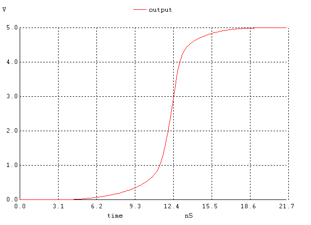
Figure 6. implementation A; the output signal when all inputs go high simultaneously.
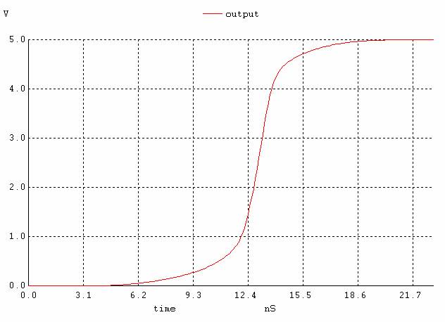
Figure 7. The output signal when all inputs except the lowest one are high and the lowest input is changing.
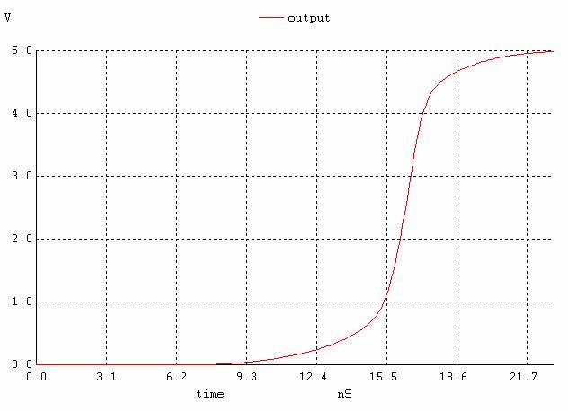
Figure 8. The output signal when all inputs except the highest one are high and the highest input is changing.
IMPLEMENTATION B
Figure 9. implementation B; all inputs changing simultaneously.
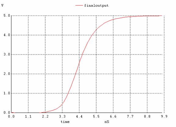
Figure 10. implementation B; the output signal when all inputs go high simultaneously.
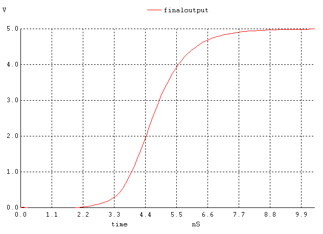
Figure 11. The output signal when all inputs except the lowest one are high and the lowest input is changing.
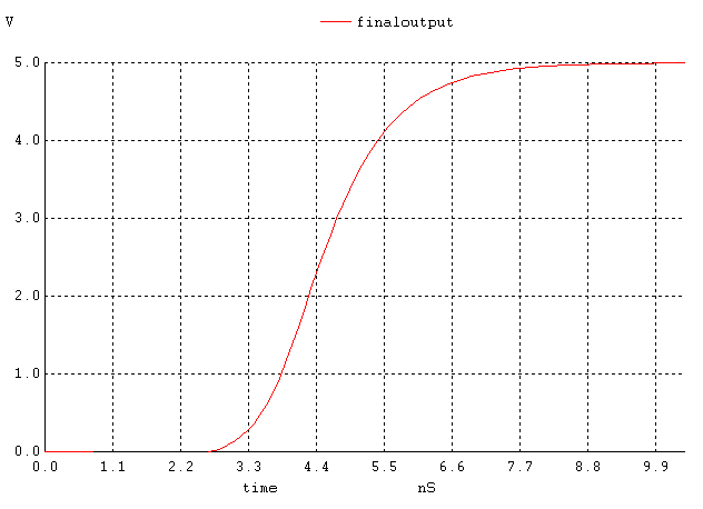
Figure 12. The output signal when all inputs except the highest one are high and the highest input is changing.
IMPLEMENTATION C
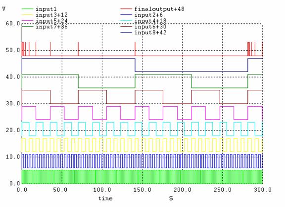
Figure 13. implementation C; all inputs changing simultaneously.
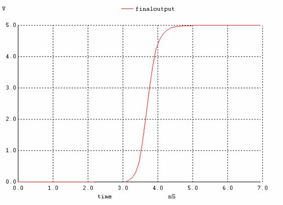
Figure 14. implementation C; the output signal when all inputs go high simultaneously.
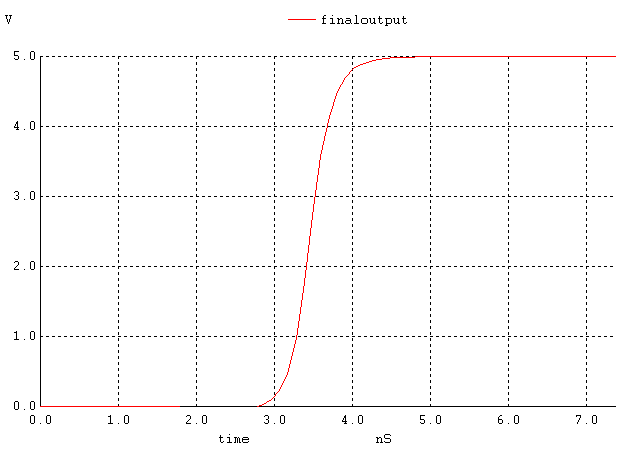
Figure 15. The output signal when all inputs except the lowest one are high and the lowest input is changing high.
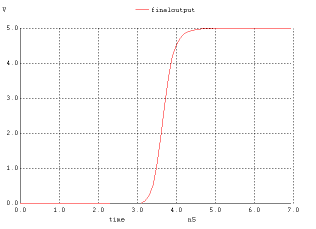
Figure 16. The output signal when all inputs except the highest one are high and the highest input is changing high.
If we compare the speeds of the three configurations (figures 6, 10, 14), we see that the output of implementation 1 starts rising at 6.7ns and settles around 22ns; the second one starts at 2ns and ends at 8.8ns and finally the third one starts at 3ns and ends at 5ns. Although the second one starts rising first (~1ns earlier than the third and ~4ns earlier than the first one), the 3rd one finishes first (~1s faster than the second and 17ns faster than the first one). See figure 17 for a comparison. Our prediction that the third implementation would be the slowest is wrong based on transistor staging, but those calculations were made assuming Cload is constant among all implementations. In implementation A, because the pulldown network consists of one large transistor, there will be greater relative to the other implementations, which are more split up. Note that the equations indicate that the larger Cload is the larger longer the propagation time. Although the other implementations have more transistor stages than A, the capacitances in them are lower and decreases propagation delay. Based on this reasoning, implementation C is faster followed by B and then A as shown in the SPICE simulation (figure 17).
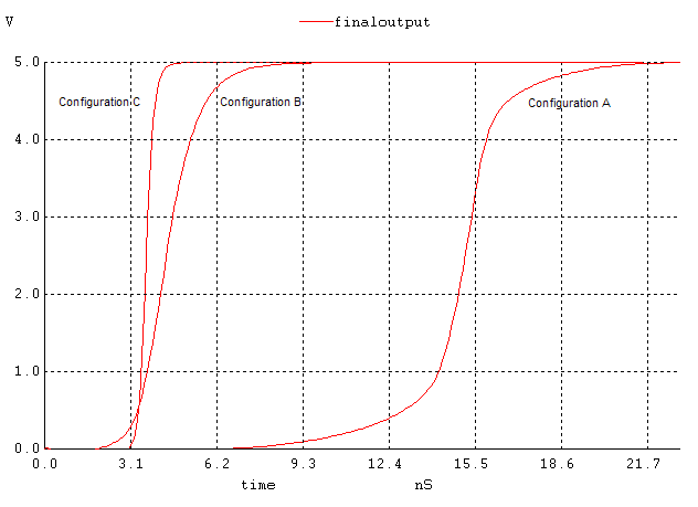
Figure 17. Comparing the speeds of the three configurations.
We may conclude that the third implementation is the best out of the three, but it takes a lot more layout space (about 4 times as much space as the first one and about twice the second one).
When we compare the start and end times of the implementations when all inputs except one of them are high and one of them is changing, we noticed that when the lowest input is changing the gates react faster. For implementation A, figure 18 shows the comparison. For the other implementations, the same phenomenon was observed. The reasoning behind this can be explained by the placement of the lowest and highest input in the layout and considering its Cload.
Toggling the highest input produces a faster output switching because it is is further down in the network and requires more time to charge and discharge it's own and neighboring transistor capacitances. The lowest input only has its own capacitance to consider because it is further up the network.
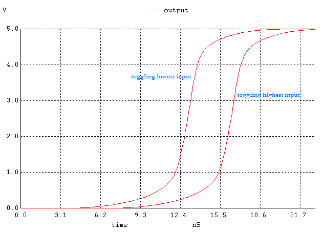
Figure 18. Alternating the lowest input vs the highest input in implementation A.
TASK 6: Do an L-Edit layout for the first implementation based on the stick figure.
As an extension, we designed L-Edit figures for all of our implementations and then extracted them to do the Spice simulations.
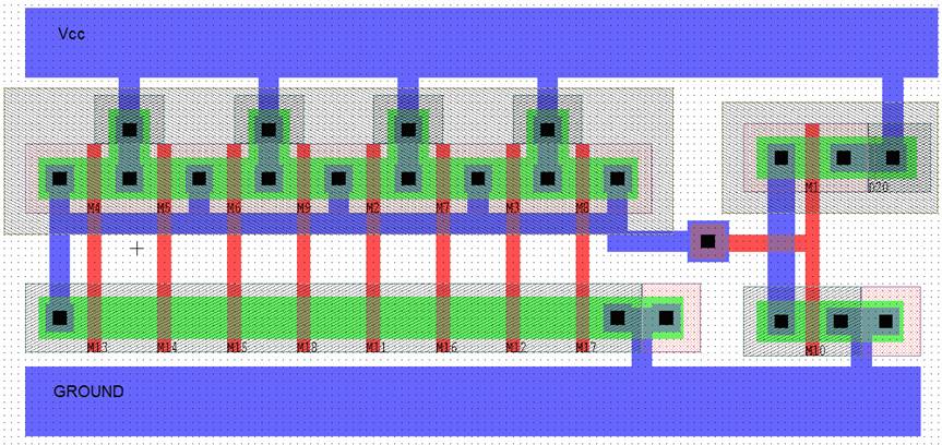
Figure 19. L-Edit figure for implementation A.
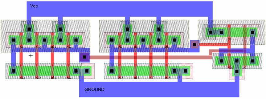
Figure 20. L-Edit figure for implementation B.
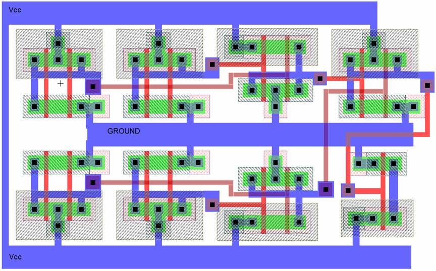
Figure 21. L-Edit figure for implementation C.
appendix.
click on the following links for the '.cir' files we used for Spice simulations [~5kb each]:
implementation A
implementation B
implementation C
The following are links to the L-edit files [~50kb each]:
implementation A
implementation B
implementation C |