abstract.
In this lab, we examined the operation of typical CMOS circuits and attemted to find the intrinsic characteristics of the transistors (VT,n and kn, and VT,p and kp) . We compared our values to those specified in the manufacturer's data sheet. Using the determined values, we modeled the basic logic gates using SPICE and MATLAB.
In addition to modelling the NAND and NOT gates, we modeled the NOR gate as an extension.
task 1.
We determined the transistor parameters for the ALD1103 by taking data from separate simple NMOS and PMOS circuits and backing out the characteristics by equation. The two circuits constructed for experimentation are shown in Figures 1a and 1b with accompanying data in Tables 1a and 1b. The test set was selected to ensure that the transistors operated in the ohmic region for purpose of later calculation. For both NMOS and PMOS transistor calculations, R was 997Ω and VDD was 5.10 V. In order to find the characteristics (VT,n and kn, and VT,p and kp) we varied the gate voltages, measured the corresponding currents through the transistors and recorded the corresponding output voltages.
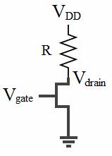 Figure 1a
. Simple NMOS Circuit |
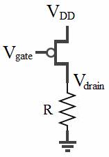
Figure 1b. Simple PMOS Circuit
|
Vgate |
Vdrain |
Iresistor (mA) |
2.09 |
0.65 |
4.329 |
2.59 |
0.44 |
4.539 |
3.54 |
0.30 |
4.679 |
Table 1a. NMOS Circuit Data
|
Vgate |
Vdrain |
Iresistor (mA) |
1.39 |
4.06 |
4.072 |
1.69 |
3.94 |
3.952 |
1.96 |
3.79 |
3.801 |
Table 1b. PMOS Circuit Data
|
VT,n and VT,p can be calculated from Equation 1 applied to two of the three data points taken. The final calculated values of VT,n and VT,p are shown in Table 2 and are the consequence of averaging the results from the three possible combinations of data points (1&2, 2&3, 1&3). Additionally, kn and kp can be calculated from Equation 2, with the final value in Table 2 being the average of the results for the three data points.
Equation 1a : 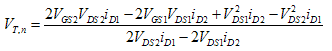
Equation 1b : 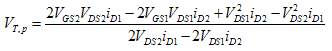
Equation 2a : 
Equation 2b : 
|
NMOS |
PMOS |
Vt (V) |
0.532 |
-0.463 |
k (mmho) |
5.49 |
1.03 |
Table 2. Calculated NMOS and PMOS Parameter Values
As a check, our device characteristics confirm the assumption in our data of operating in the linear region of the transistors. We feel our methodology is valid for a good approximation of parameters because we utilize averages to help reduce the effects of variability. For more accurate numbers, the size of the data set should simply be increased. Table 3 shows the range of nominal values from the manufacturer’s datasheet for both Vt and k.
|
Vt,min |
Vt,typ |
Vt,max |
kmin |
ktyp |
NMOS |
0.4 |
0.7 |
1 |
5 |
10 |
PMOS |
-0.4 |
-0.7 |
-1.2 |
2 |
4 |
Table 3. ALD1103 Data Sheet V t Values
The majority of our experimental values compare favorably by falling within the specified ranges. However, our kp value is surprisingly low, but not completely unreasonable. Figures 3 and 4 show the comparison between the SPICE simulations and experimental data.
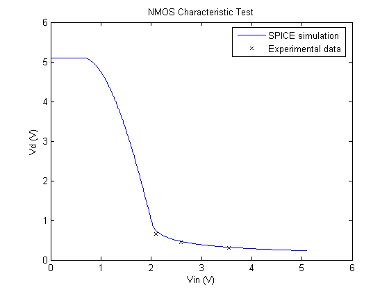
Figure 2. Comparison of NMOS characteristics.
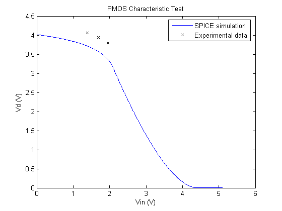
Figure 3. Comparison of PMOS characteristics.
Our NMOS characteristic measurements match quite closely with the SPICE simulation. However, our PMOS data points, though correct in shape, appear to be offset from the theoretical simulation. We believe that this is partly attributed to the fact that the vertical positioning of the curves is affected significantly by VT,p, and our SPICE and measured values are dissimilar.
task 2.
Using the same transistors we used in task 1, we experimentally determined the transfer characteristics of the CMOS inverter. Then we compared these values with theoretical values we derived and with SPICE model transfer characteristics.
Here's out methodology for devising the theoretical transfer characteristics of the inverter. Figure 4 shows the regions the inverter operates in, allowing us to plot Vin vs Vout.
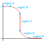
Figure 4 . Inverter operation regions.
Region A: nMOS is in cutoff and pMOS is in linear so we have Vout = Vdd.
Region B:
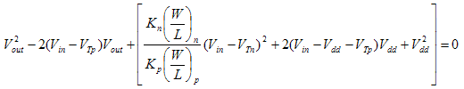
Rewriting in terms of Vout, Vin and Vdd we get:

This equation simplifies to:
Letting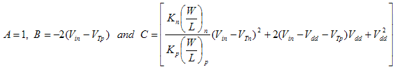
We have 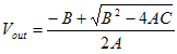 . Notice that the coefficient of . Notice that the coefficient of  is +1, the negative coefficient yields unrealistic results. is +1, the negative coefficient yields unrealistic results.
Region C:
pMOS and nMOS are both in saturation so we have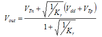
Notice that this region will be vertical since channel length modulation is ignored. (Kr=Kn/Kp)
Region D: nMOS is in ohmic, pMOS is in saturation. We have:
Rewriting the equation in terms of Vout, Vin and Vdd we get:

We have another quadratic equation;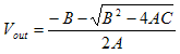 where where

Notice that this time, the coefficient of is -1; the positive coefficient yields unrealistic results.
Region E: nMOS is in ohmic and pMOS is off therefore we have Vout = 0V
Our SPICE simulation can be found here.
We transferred our results from SPICE and our experimental results to MATLAB and we used MATLAB to plot the comparison of theoretical, simulation and experimental values. The simulation is based off of the datasheet values of the transistors. The plot can be seen in Figure 5. Here is the m-file we used.
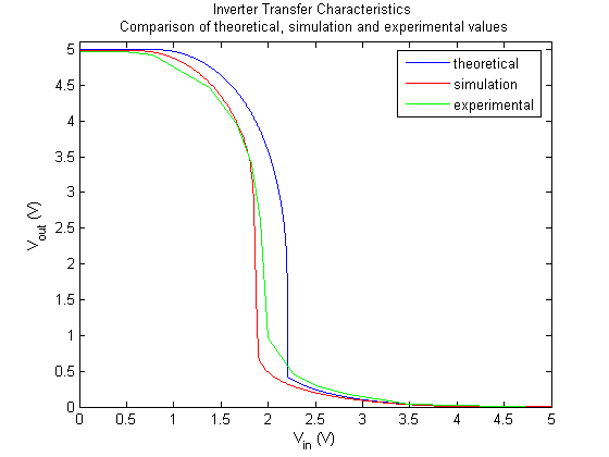
Figure 5. Inverter Transfer Characteristics.
The theoretical, simulation, and experimental curves all seem to relate fairly well as we would hope.
task 3.
In this section we modeled basic logic gates using CMOS transistors. These logic functions are built from the basic inverter. By inspection, this can be observed by looking at Figures 6a and 6b. This feature allows for a similar analysis for the transfer characteristics performed for the transistor. In the NAND gate, a parallel PMOS transistor is added in upper network and a NMOS in series in the lower part. Similarly the dual action is done for the NOR gate.
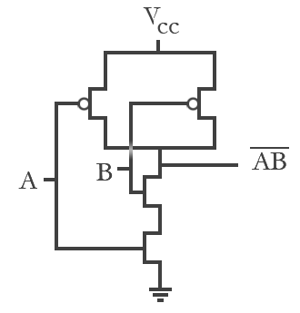 Figure 6a
. NAND gate schematics |
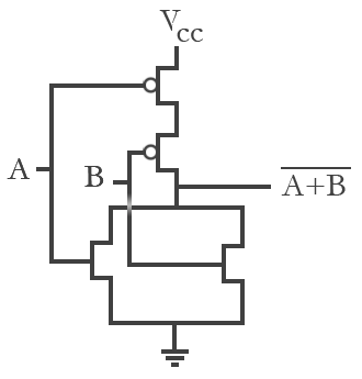
Figure 6b. NOR gate schematics
|
NAND gate |
A |
B |
output |
0 |
0 |
1 |
0 |
1 |
1 |
1 |
0 |
1 |
1 |
1 |
0 |
Table 4.
NAND gate logic function |
NOR gate |
A |
B |
output |
0 |
0 |
1 |
0 |
1 |
0 |
1 |
0 |
0 |
1 |
1 |
0 |
Table 5.
NOR gate logic function |
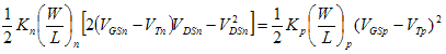
In the analysis, the only difference is to account for the appropriate change in channel width and length for each configuration to find the equivalent inverter layout. Two transistors in series serve to double the length while two in parallel double the width. This induces doubling or halving the kp and kn found in task 1.
SPICE simulation and theoretical analysis in MATLAB were used again to validate the experimental data. We performed three cases to test the logic functionality, and note dynamic differences. These are summarized as the following for the NAND (NOR) gate: 1) holding input A high (low) while varying B, 2) holding input B high (low) while varying A from 0 to Vdd, and 3) tying both inputs and varying from 0 to Vdd.
The graphs shown below present our results sequentially. For both the NAND and NOR gates, experimental and SPICE transfer characteristics are contrasted for the three test cases. The theoretical method is included in the last graph along with the previous two graphs for group analysis.
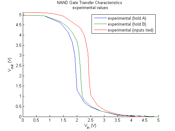
Figure 6. NAND gate experimental transfer characteristic results
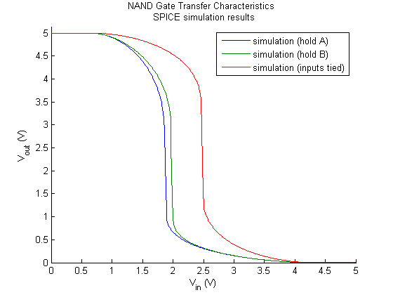
Figure 7. NAND gate SPICE simulation results.
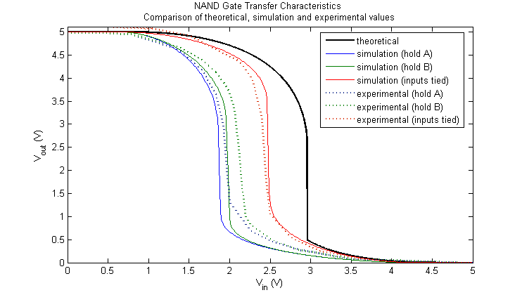
Figure 8. Comparison of NAND gate transfer characteristics
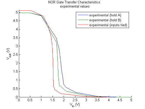
Figure 9.
NOR gate experimental transfer characteristic results
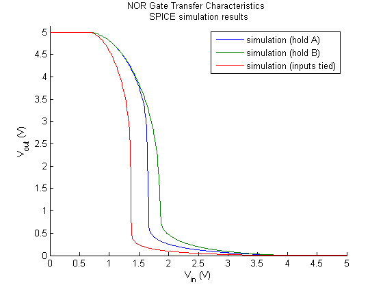
Figure 10. NOR gate SPICE simulation results.
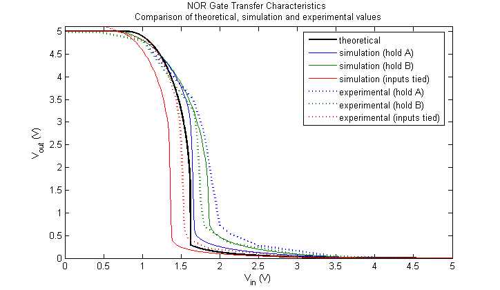
Figure 11. Comparison of NOR gate transfer characteristics
The relative positioning of these graphs make sense in terms of a Vth analysis (Refer to Task 2, Region C for the exact equation for Vth). In the case of NAND, the value of kp halves and the value of kn doubles, increasing the value of kR by four times. This serves to reduce the overall threshold voltage as compared to a tied-input inverter arrangement as seen in Figure 8. The opposite is true in the case of NOR where kp doubles and kn halves, and the value of kR is reduced by four times. As expected, Figure 11 shows that the threshold voltage is generally greater than the tied-input inverter case.
The logic gate operates as expected. The output is only low when the varying input is high. Note the difference depending on which input is varied. Because input B has to charge and discharge its own capacitances and that of input A, varying B experiences a higher propagation delay and thus a slower switching speed.
As an extension we explored the dynamics of the NOR gate and discovered similar switching dynamics. We held one input low instead to watch the switch from high to low. Because the NOR gate is built from a CMOS inverter configuration, it is not surprising to see a similar switching dynamic. The same is true for the NAND gate.
The same transfer characteristic method is used for these two gates. With the appropriate changes to kn and kp in the MOSFET drain current equations, the inverter analysis still applies. Because the PMOS network in the NAND gate sees an extra transistor in parallel, the change is a transistor with an effective channel width doubled. The original kp then doubles. An additional nMOS transistor in series then sees a doubled channel length, and hence a halved kn. The opposite argument can be made for the NOR gate.
Figures 8 and 11 show the comparison of transfer characteristics between theoretical, experimental and simulation results.
|