|
abstract
in this lab, we implemented an analog to digital converter circuit. the first part of our circuit took the output of a photocell and amplified it to a working range of 0 to 5 volts. this signal was then sent through a low pass filter to remove excess noise. we then converted the filtered analog signal it to a digital signal, which was relayed through parallel communication to 7-segment display.
transducer overview
as stated above, the transducer that we decided to use was a photocell, shown in figure 1. the photocell produces a voltage across its terminals that is directly proportional to the amount of light that the sensor sees. in other words, as the amount of light that enters the sensor increases, the voltage across the terminals of the sensor goes up.
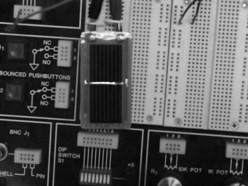
figure 1. a photocell.
task 1 . the a/d converter circuit [transduction and amplification]
this part of the lab was put together entirely on a breadboard. the positive and negative outputs of the photocell were sent directly to the inputs of a 741 operational amplifier. in order to magnify the input signal to the desired 0 to 5 volt range, we set the operational amplifier circuit up in a non-inverting configuration, as shown in figure 2. the circuit as it appeared on the breadboard is shown in figure 3. the gain of this configuration is given by G = 1 + R2/R1. we used resistors with values of R1 = 15E+2 and R2 = 56E+3 to achieve a gain of 38.3, which resulted in an output signal ranging from 0 to about 4.8 volts (observed by connecting the outputs of the operational amplifier to an oscilloscope).
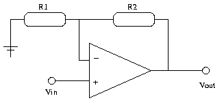
figure 2. the noninverting amplifier circuit.
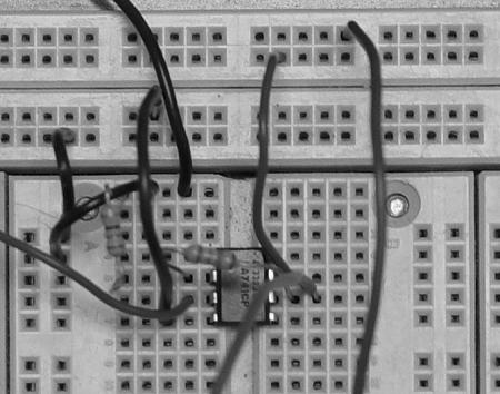
figure 3. the noninverting amplifier circuit, implemented.
task 1 . the a/d converter circuit [low pass filter]
the next step was to clean unwanted noise out of the date by applying a low pass filter to the analog signal. we used a simple combination of a resistor and a capacitor to accomplish this, as depicted in figure 4. we wanted the cutoff frequency of the filter to be equal to a little more than twice the signal frequency (in accordance with the niquist criterion). according to the specifications of the a/d converter that we were going to use, its clock frequency was 640 khz. given that the altera board samples its inputs at approximately 64 hz, we knew that our rc combination had to satisfy the relationship RC = 2E-4 seconds (we knew that 1 / RC = (640 khz / 64) / 2). we chose the values R = 200 ohms and the corresponding C = 1 microfarads.
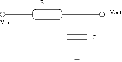
figure 4. a simple low pass filter.
task 1 . the a/d converter circuit [analog to digital conversion]
at this point, the processed analog signal was ready to be converted to a digital signal. we used an adc0804 converter, and connected the pins as specified by the component's specification sheet. we connected the outputs of the chip to the test led's on the breadboard to determine whether the a/d converter was working as desired.
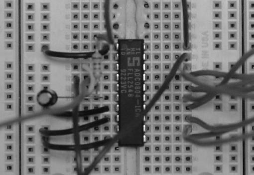
figure 5. the a/d conversion circuit.
task 2 . communication [initial test]
the next thing that was done was to interface this breadboard circuitry with the altera board, which would accomplish the communication task. as a first test, we programmed the board to take an eight bit input and display it on the 7 segment display (done simply using eight_to_seven.vhd, which had been written prior to this lab). this gave us a nice readout, and we could tell that the transduction, processing, and a/d conversion were working correctly.
task 2 . communication [nibble communication]
the final part of the procedure was to implement a nibble mode parallel communication on the altera board. nibble mode is a form of data communication in which a string of data is sent between a host and a peripheral in segments rather than all at once. a timing diagram for nibble communication is shown in figure 6.
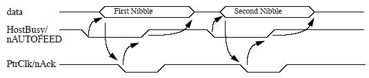
figure 6. nibble communication timing diagram.
in this case there are eight bits of information to be sent; each nibble consists of four bits. consequently, each nibble is represents one digit on the altera board's seven segment displays. the communication was implemented by the code found in nibble.vhd. this program uses the same eight_to_seven.vhd to output the data collected by the host on the altera board's seven segment display. it is an implementation of the state diagrams drawn in figures 7 and 8.
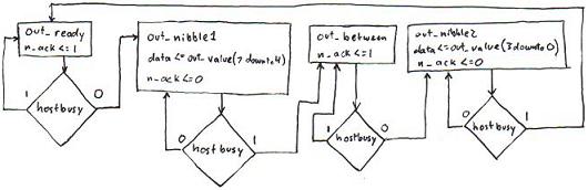
figure 7. parallel out state diagram (peripheral).
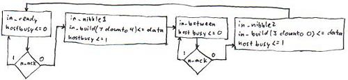
figure 8. parallel in state diagram (host).
as can be seen in the figures 6, 7, and 8, this nibble communication is accomplished with only 6 parallel data lines running from the host to the peripheral. the 'hostbusy' line is set high by the host when it is in the process of reading data, and then is set low again when the host has completed reading. the 'n_ack' line ('n_' meaning active low) is set low by the peripheral when there is data on the data lines that is ready to be read. this signal is then set high again when the host signals that it has read the data, and is set low once again when the next nibble is ready to be read.
combining tasks [the final circuit]
once both task one and two were completed, the two parts were combined to produce the completed project. the project is shown in figure 9.
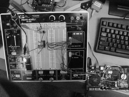
figure 9. the completed project.
extension [peak holder]
after combining tasks one and two to produce the final circuit, we decided to give our device increased functionality. using the code found in nibble_peak.vhd, we gave our circuit the option of holding it's peak value; if the user holds a pushbutton, then the display will show the maximum value inputted from the analog circuit over the duration of the button press.
in this case, we set one of the pushbuttons on the altera board as an input to the host. when pressed, the host went into an alternate routine in its in_nibble states; the host would only accept and store values that were higher than any previous values during the button press. the algorithm for determining whether or not to keep a new value was based on the fact that each nibble represents one of the numbers on the seven segment display. in the code, it can be seen that the more significant digit was recieved first. the tricky part of this task was to account for the fact that if the more significant digit increases, then the less significant digit can decrease (for example, 71 is greater than 68). this concept was put into our code by letting the host set a flag if the significant digit increased. then, when the host recieved the less significant digit, it accepted the new value automatically if the flag had been set. if the flag had not been set, then the host only accepted values higher than the current state of the digit.
conclusions
by completing this lab, we learned how to implement a basic sensor system. using the output of a transducer, we learned how to process the signal such that it could be sent into an analog to digital signal converter. given the digital output of the converter, we gained more experience with developing code for parallel communications. although we did not have the option of networking a true host with our peripheral, we were able to simulate such an interaction on the altera board.
|