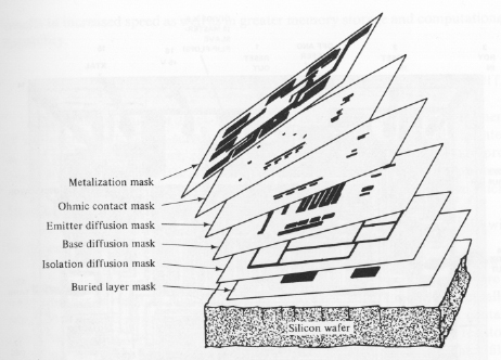
Figure 2: Series of photo masks. The light used in EBL is very intense so that exposure can be quite short. Since a typical mask can be few inches in square, and since electron beams can be deflected over only a small angle without distortion, a complete mask is made by repeating a given design until the entire mask is exposed. Electron beam exposure is rather slow because of its low energy and relatively insensitive resist. But because the diffraction effects of electrons are much less than that of lights in photolithography, EBL is the preferred method when high-resolution masks are desired. Advantages of EBL process include smaller line - width, thus producing high-quality masks, and provide simple modification process by altering the computer data file containing the design. Before resist can be exposed, mask alignment must be carefully checked and rechecked to avoid circuit defects. The accuracy of alignment generally includes marker matching between levels. The three basic types of mask aligners are contact, off-contact, and projection printing. In contact alignment, the mask is placed directly on top of the wafer and it is either aligned manually or automatically. Then the wafer is vacuum clamped tightly with the mask. After rechecking alignment and it is found to be satisfactory, resist exposure is carried out. In off-contact alignment, there is a 5 to 30 um separations between wafer and mask. The lack of contact reduces the wear on the mask but at the same time making accuracy more difficult to achieve. Due to possible warping of wafer, great care must be taken to ensure the wafer is flatten and that the wafer is almost perfectly paralleled to the mask. In the projection printing approach of mask alignment, an image of the mask is literally projected onto the wafer using either transmitting or reflecting optics. Its performance is similar to off-contact alignment concerning mask wear. In the case where transmitting optics are used, the process must use monochromatic light source to minimize chromatic aberration. In doing so, it requires a longer exposure time and is also subject to the negative effects of interference layers in negative photoresists. The interference layer is the result of either constructive or destructive interference of light when it is reflected from the top of the oxide and silicon surface. Constructive interference occurs if the path-length difference is a multiple of the wavelength, whereas destructive interference occurs at odd integral multiple of the half- wavelength. The phenomenon reduces edge definition since during the rinsing process, some of the unexposed resist will tend to be removed. On the other hand, the reflective optical process can avoid the problem of chromatic aberration. The first resists used in semiconductor fabrication process were of negative type in which negative images were produced. Solvents can remove resist layers unless they are exposed to ultraviolet light. In the fabrication of large-scale integrated circuits, use of positive resists is preferred over negative resists. The positive resists have shorter polymer links and therefore easier for the solvent to break up. A higher resolution of the circuit design is achieved with a thinner resist layer. But the draw back is its higher density of pinholes. Therefore, the modern lithography process usually employs two layers of resists for design exposure. Positive resists are also in use later on. A different chemical based solvent is used to remove regions that have been exposed to light, rather than regions that have not been exposed. The two different types of resists that you would mostly likely encounter in fabrication are photoresists and electron resists. Traditionally, the contact alignment process is used to achieve a small line width of 2 um within the tolerated diffraction around the edges of mask patterns. As mentioned earlier, direct contact causes damage to the wafer and mask. The development of laser interferometry was able to improve the tolerance by using projection printing.