The bonding and packaging of an integrated chip provide connections to the
outside world. Usually, an IC can be packaged individually or incorporated
into a hybrid circuit. Packaging the circuit give it some mechanical and
environmental stability. Additional tests are carried out for chip electrical
and mechanical behaviors after it is packaged. The two common bonding techniques
are thermocompression bonding and ultrasonic bonding.The following is a
discussion of ball bonds and stitch bonds.
Gold is often used as interconnection material because it is easy to weld to
silicon by applying enough heat and pressure simultaneously. In order to
achieve tight contact between the bonding surfaces in thermocompression bonding,
a very small mechanical scrubbing action is used. Generally, the process takes
place in a nitrogen environment to prevent oxidation. One of the most often used
equipment for thermocompression bonding is the nail-head bonder (See Figure 4).
First, a gold wire with a sphere at its head is fed through the capillary. It
is then lowered after being aligned with the bonding pad on the die. To form a
connection, the god sphere is pressed against the die for few seconds to form
a weld. The temperature during the process is maintained at
around 300 Celsius. After connection is established on the bonding pad of die,
the capillary raises the gold to form a lead. Finally a hydrogen torch is used
to break the wire.
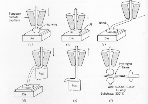
Figure 4: Precedures for making a ball bond.
The alternative to ball-bonds is stitch bonds. The process is similar (see
Figure 5), and the bond is made by either by applying heat and pressure or
ultrasound energy. The wire is fed through the capillary the wedge tool. The
tail of the wire extends from the hole and is placed parallel to the bonding
surface. Pressure from the wedge forces the wire onto the bonding pad. The setup
is similar to the making of a ball bond. In general, the nail-head bonder that
makes ball bonds has been found to be considerably faster and results in stronger
bonds.
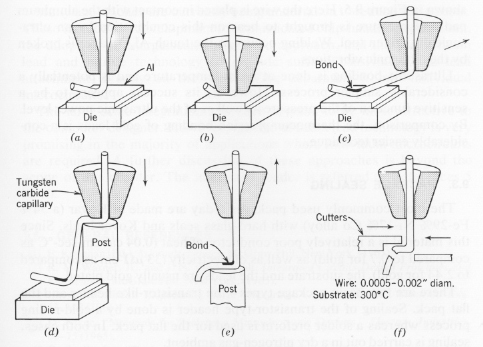
Figure 5: Precedures for making a stitch bond.
A few of the common packaging format for IC chips are dual-in-line package (DIP),
TO-can types, and flat packs. DIPs are most popular among others. They are easy
to handle and convenient to use in printed circuits. The socket of DIPs can be
made from ceramic or plastic. Ceramic DIPs have a gold-plated ceramic substrate
for chip attachment. Either glass or epoxy seals the lid. The TO-can types have
the die bonded on a gold-plated header. The cap is then attached by resistance
welding. It is at this stage that the concept of mass production breaks down. Once
chips are separated into individual pieces, the production cost is very large.
Therefore, packaging micro-circuits takes up a major fraction of over-all cost
of manufacture.
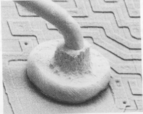
Figure 6: A ball bond made by thermocompression.
|
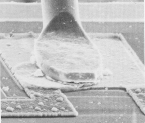
Figure 7: A stitch bond made by ultrasound.
|