
In this lab we used switched capacitor circuits to implement low pass, high pass and band pass analog filters. The switched capacitor is very useful in that it doesn't require resistors. In integrated circuits, resistors take up a lot of space and are avoided as much as possible so switched capacitors have many uses in integrated circuits.
For our lab, we used the LMF100, a chip that can be used to implement two second order filters or a fourth order butterworth filter.
Click here to see the lab procedure. (80 kb word document)
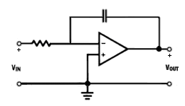
Figure 1. typical integrator
The circuit in Figure 2 can be used to build the three filters we implemented using the LMF100. The integrators are simplified and you can assume they are the integrator shown in Figure 1.
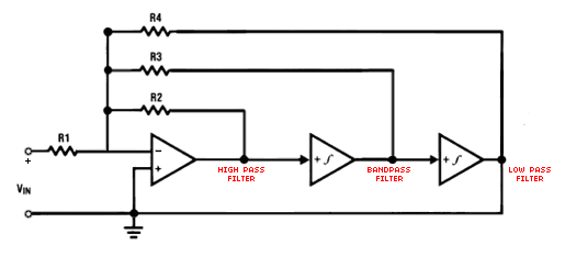
Figure 2. Implementation of high pass, low pass and band pass filters.
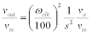
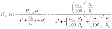
In the following derivations we will be using the circuit shown in Figure 2 and we will assume ω0 is 1/100th of the clock frequency.
Let's call the voltage at the inverting input of the first op-amp va. Then summing all currents into the same node yields the following:
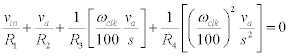
If we simplify this equation, we get:
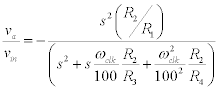
For the low pass output we have:
So,
Then,
 and and 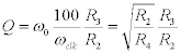
The equations for the other filters can be derived similarly.
For the first part of the lab, we are required to have a center frequency of 500Hz and a 200Hz bandwidth (Note that the bandwidth is the region where the gain is higher than 70.7% of the maximum gain) Then:
Q= f0/B =500/200=2.5
We would like to set R1= R4so that the square root term will be 1. Then, using a clock speed of 50kHz, from the equation of Q (see equation above), we need to have R3/R2=2.5
In our circuit, we decided to use R1= R2= R4=20kΩ and R3= 50kΩ. Given these resistor values here are the equations and corresponding gains:
You can see our final design using the LMF100 in Figure 3.
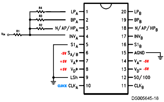
Figure 3. Implementation of filters using the LMF100.
(Acknowledgement: the picture of the LMF100 in the figure above was taken from the data sheet and modified to represent our circuit)
After setting up our circuit we took measurements with ω0=ωclk/100 and ω0=ωclk/50. Table 1 shows the gains of the filters using ω0=ωclk/50.
Frequency |
Low Pass
Gain |
High Pass
Gain |
Band Pass
Gain |
| 1 |
1 |
0.01 |
0.01 |
| 10 |
1 |
0.01 |
0.01 |
| 100 |
1 |
0.05 |
0.2 |
| 200 |
1.1 |
0.15 |
0.4 |
| 250 |
1.2 |
0.2 |
0.5 |
| 300 |
1.3 |
0.4 |
0.75 |
| 350 |
1.5 |
0.65 |
1 |
| 400 |
1.75 |
1 |
1.3 |
| 450 |
2.2 |
1.5 |
1.8 |
| 500 |
2.4 |
2 |
2.4 |
| 550 |
2.2 |
2.4 |
2.4 |
| 600 |
1.8 |
2.25 |
2 |
| 650 |
1.35 |
2 |
1.6 |
| 700 |
1.1 |
1.75 |
1.4 |
| 750 |
0.8 |
1.6 |
1.2 |
| 800 |
0.65 |
1.5 |
1 |
| 900 |
0.55 |
1.3 |
0.8 |
| 1000 |
0.35 |
1.25 |
0.6 |
| 1200 |
0.2 |
1.1 |
0.5 |
| 1500 |
0.1 |
1 |
0.4 |
| 2000 |
0.07 |
1 |
0.3 |
| 4000 |
0.035 |
1 |
0.15 |
| 10000 |
0.02 |
1 |
0.1 |
Table1. Gains of the filters using ω0=ωclk/50.
Figure 4 shows the gains (both axes are logarithmic) of the filters for the first set-up. Notice that the center frequency is 550Hz, which compares very well with our expected frequency of 500Hz. It is a little hard to read from the graph but the 70.7% cutoff is between about 450Hz and 650Hz, which again is very good in terms of our initial expectations. Looking at Table 1 and Figure 4 we see that HOLP=1V/V, HOHP=1V/V and HOBP=2.4V/V. The first two values are just what we expected, however the high output for the band-pass filter is slightly lower than our projected value of 2.5kHz.
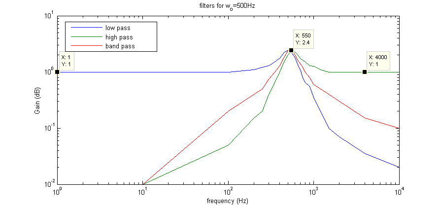
Figure 4. Gains for filters at ω0=500Hz.
In the second set-up, we used ω0=ωclk/100. Table 2 shows the gains.
Frequency |
Low Pass
Gain |
High Pass
Gain |
Band Pass
Gain |
| 1 |
1 |
0.01 |
0.1 |
| 100 |
1 |
0.03 |
0.2 |
| 200 |
1 |
0.08 |
0.33 |
| 400 |
1.2 |
0.2 |
0.55 |
| 500 |
1.3 |
0.4 |
0.75 |
| 600 |
1.5 |
0.66 |
1 |
| 700 |
1.75 |
1 |
1.3 |
| 800 |
2.2 |
1.5 |
1.8 |
| 900 |
2.4 |
2 |
2.33 |
| 1000 |
2.2 |
2.4 |
2.4 |
| 1100 |
1.8 |
2.25 |
2.1 |
| 1200 |
1.35 |
2 |
1.6 |
| 1300 |
1.15 |
1.8 |
1.4 |
| 1400 |
0.82 |
1.6 |
1.2 |
| 1500 |
0.68 |
1.5 |
1 |
| 1600 |
0.56 |
1.33 |
0.8 |
| 1800 |
0.33 |
1.25 |
0.6 |
| 2000 |
0.22 |
1.1 |
0.5 |
| 2400 |
0.12 |
1 |
0.4 |
| 3000 |
0.07 |
1 |
0.33 |
| 4000 |
0.035 |
1 |
0.15 |
| 8000 |
0.02 |
1 |
0.1 |
| 10000 |
0.01 |
1 |
0.1 |
Table2. Gains of the filters using ω0=ωclk/100.
In all of our readings, the gains were almost identical to the first set-up. In fact, you can see that most of the time, the gains for a particular frequency in part 2 match the gains for half that frequency in the first part.
In the second part, the center frequency was slightly lower than 1kHz. For clarity we took measurements at certain frequencies but in lab, we noticed that the peak gain occured around 975Hz. However, it wasn't much higher than 2.4V/V. Looking at Table 2 and Figure 4, we see that our results compare really well with expected results, but the peak gain is again slightly lower than 2.5V/V. This could be due to the fact that resistors aren't perfectly at 20kΩ and 50kΩ. Also, the gains for low frequencies with the low pass filter and high frequencies with the high pass filter weren't exactly 1, but they matched to within 1% of a unity gain. for all practical purposes this can be considered a unit gain.
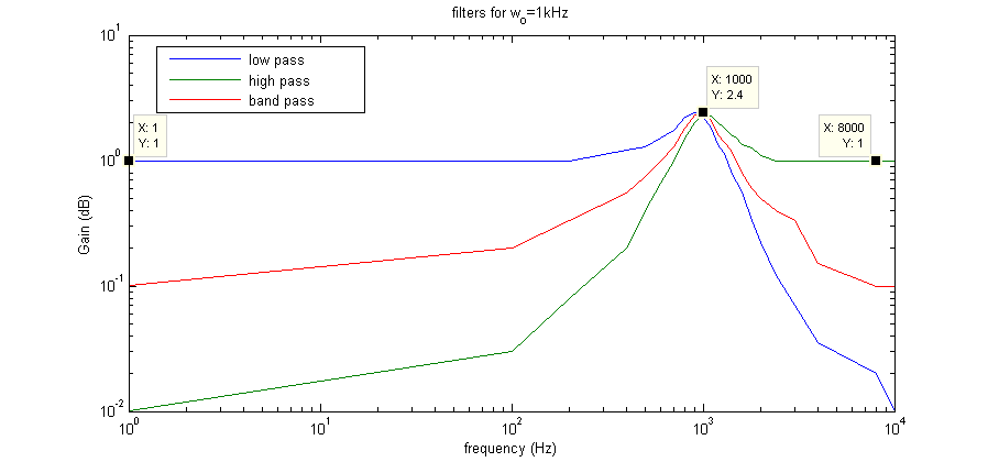
Figure 5. Gains for filters at ω0=1kHz.
We were lucky to get a discrete output. See Figure 6
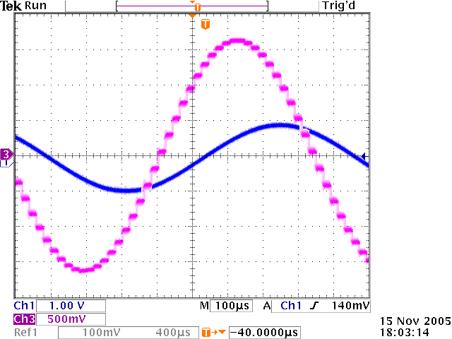
Figure 6. Discrete steps in the output.
|