|
In this lab, we primarily focused on the operation of bipolar junction transistors. We looked at the common emitter amplifier and starting from basic versions, we built more efficient circuits. We also looked at voltage regulators and improved regulators from our previous labs using transistors. Finally we looked at a pumped op-amp and made slight modifications to improve performance.
In order to make reading this lab easier, the lab procedure and out work are integrated. you can find the full lab description at Prof Erik Cheever's website.
The parts taken from the lab website have grey backgrounds.
| bipolar transistor basics. |
Note: this section is taken from Prof Cheever's website.
Transistors are a bit more complicated than diodes in that they are three terminal devices. The transistors we will be using are called bipolar transistor (in contrast with field effect transistors, or FETs, that you will see later in the semester) and come in two flavors NPN and PNP. On an NPN transistor the arrow is Not Pointed iN.
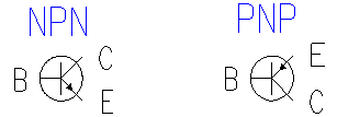
As you can see the two transistors look very similar. They have three terminals the Base, the Collector and the Emitter, labeled B, C and E in the drawing. As with the diode there are many different models for the transistor. The models we are going to use are shown below.
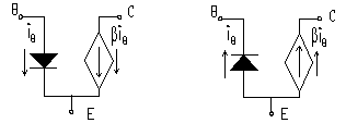
Consider first the NPN transistor shown at the left. If the base is at higher (@0.6 volt) potential than the emitter then a current iB will flow into the base. The current into the collector is b times larger than the base current. The quantity b (usually called hFE in transistor spec sheets) is a characteristic of the individual transistor and is typically in the range from 100-500 for the types of transistors we will be using. The emitter current is the sum of the base and collector currents, but since the collector current is so much larger than the base current it is common practice to equate the collector and emitter currents. Thus the transistor can be thought of as a current amplifier device -- the current at the output (collector or emitter) is b times large than the current at the input (base). However you should be aware of shortcomings of this model:
This model begins to fail when the collector voltage is approximately equal to the emitter voltage (actually vC-vE=vCE@0.2volts). At this point the device no longer continues to amplify the signal. This condition is called saturation.
If the voltage at the base is too low to turn the base-emitter diode on, then there is no current. This condition is called cutoff.
We can now define the three regions of operation for the transistor:
Saturation (vCE@0.2volts, vBE@0.6 volts). This is also called the "on" state.
Active region (vCE>0.2 volts, vBE@0.6 volts). In this region ic= bib. This is also called the linear region.
Cutoff (vBE<0.6 volts). No current flows. This is also called the "off" state.
When the transistor is to be used as a switch, it is used either in cutoff (switch is off, or an open circuit) or saturation (switch is on, or very close to a short circuit). When the transistor is to be used as an amplifier the transistor is kept in the linear regime (neither cutoff nor saturated), and acts as a current amplifier.
The PNP transistor is very similar to the NPN transistor except:
The base is at a lower voltage than the emitter to turn the transistor on.
he current flows out of the base and collector and into the emitter. The direction of current still follows the direction of the arrow.
t saturation vE-vC=vEC@0.2volts.
For both the NPN and PNP transistor:
The arrow represents a diode between the base and the emitter.
iC=biB if the transistor is not in saturation.
The currents in the transistor follow the arrow (NPN -- from base to emitter and from collector to emitter. PNP -- from emitter to base and from emitter to collector).
The arrow is on the emitter.
The procedure section shows a variety of transistor applications
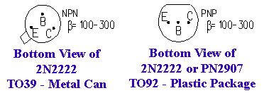
The two types of transistors that you will be using are shown in the diagram below. The PN2907 is in a plastic package, the 2N2222 may be either plastic or metal. Note that the view is from the bottom, and that one of the transistors is NPN and one is PNP. Link to: 2N2222 datasheet, PN2907 datasheet.
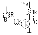
Measuring b
1) Use a 2N2222 transistor and connect the circuit shown below. Measure ic and ib for several values of R from 0 to about 1 MW. This is most easily done by measuring the voltage across the 1kW and 10kW resistor and calculating the currents. Don’t take a lot of measurements when the voltage across the 1kW resistor is near 15 volts, because this indicates that the transistor is saturated (vce@0.2V). Estimate b from the measurements taken when the transistor is not saturated (voltage across 1kW resistor is less than about 14.5 volts).
|
Graph base current vs collector current. Identify the linear region of operation and calculate a value for β. Also identify any data that are in the saturation or cutoff regions.
In order to find β we plotted the values of ic versus ib. The slope of the line gives us β. Figure 1 shows the graph of ic vs ib. In order to get the actual value of β we need to look at the linear region (ie. the non-flat portion of the plot) Figure 2 shows the linear region and the best fit line. β ≈ 113.
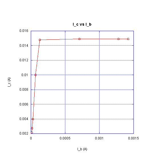
Figure 1. ic vs ib.
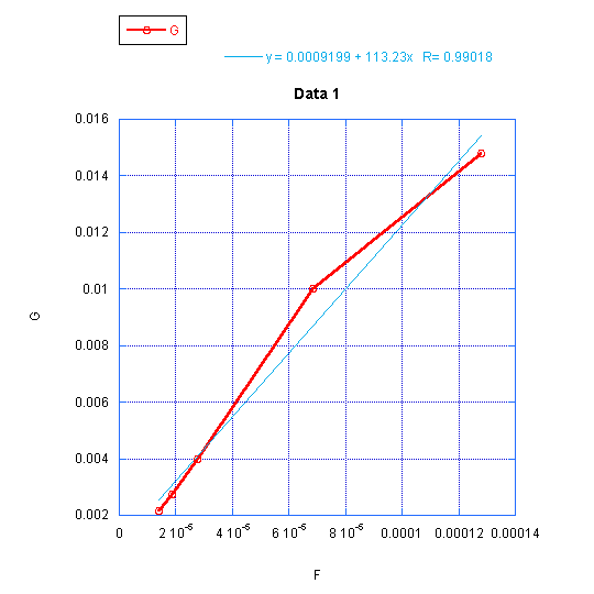
Figure 2. ic vs ib : linear region and the best fit line. (β ≈ 113)
The Common Emitter Amplifier.
A first attempt at a transistor amplifier.
Now consider what would happen if we built the circuit shown below.
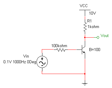
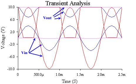
In this circuit the input is so small that the transistor never turns on and the output is at 10 volts.
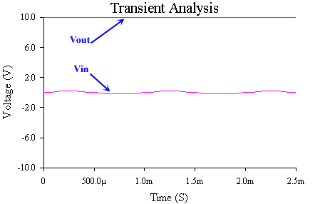
Clearly this is not a very good amplifier. To turn the transistor on we can increase the magnitude of the input voltage. When the input is above 0.7 the transistor starts conducting, current flows and the voltage drops. Making the input a 4 volt (8 V p-p) results in the blue lines on the image below. Increasing it even more results in the output being clipped on both its positive and negative peaks.
An improved amplifier - biasing.
Obviously our first attempt at a transistor amplifier was unsuccessful because we were operating in the non-linear regions of the transistor characteristics. Consider, instead, the circuit shown below in which a DC source is added in series with the input. The DC source acts to ensure that the transistor is always on and in the linear region (as long as the input is small enough). To think about what is happening consider that even when the input is zero, current is flowing in the transistor so it is in the linear region. This is referred to as biasing the transistor. Now if we add the sinusoidal source this will simply increase or decrease the amount of current through the transistor.
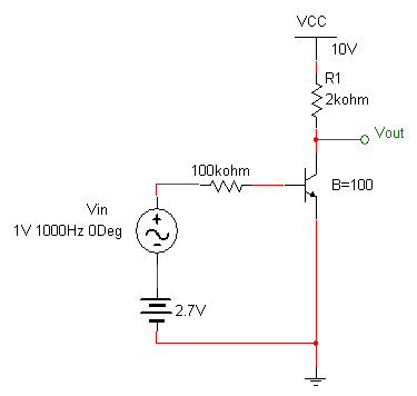
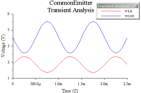
The input and output are shown below. We have created a working amplifier, but lets consider some practical problems with this design.
A Simple Common Emitter Amplifier
The biasing scheme used above is generally impractical because many signal sources are not capable of generating a DC offset for a sinusoidal signal, so we need to bias the transistor another way. We will do this by lowering the voltage on the emitter.
2) Build the circuit below and predict, then measure, the DC current into the collector. You can use an ammeter to do this, but it is easier to measure the voltage across the 2k resistor, and use that to find the current through it. To measure DC voltages you can simply take out the sinusoidal source. You may assume that the base current is small which greatly simplifies calculations.
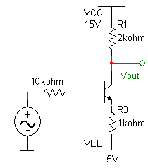
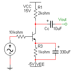
Biasing with a negative supply
|
Calculate the DC currents in the circuit. Verify your calculations with measurements from your circuit. Explain, in your own words, the need for biasing.
For DC analysis, we ignore the input signal in the figure above (assume the input signal is 0). In lab, our values for resistors and sources were as follows:
VCC= 15.1 V
VEE= -5.1 V
R1= 2.01kΩ
R2= 9.98kΩ
R3= 997Ω
We can now do our analysis.
Keeping in mind that VE=VB=VBE we have the following:
This yields VB= -0.3552 V
We conclude that VE= -1.0552
iE = (VE-VEE)/997Ω = 3.96mA
Then iB=0.347mA and iC=3.92mA. These values mean the voltage drop across R1should be 3.92 x 2.01 = 7.88 V. The experimental value we found was slightly higher, 7.94V but for all practical purposes these values match really well.
3) Next connect the source, with the DC offset turned off, and the frequency set to about 10 kHz. Turn it on and observe the output when the input is adjusted so that there is no distortion in the output. Note that the output has a DC offset. Make sure you can explain how this circuit works. Print out an oscilloscope image that clearly shows the input and the output, including the DC offset of the output.
|
Is this DC offset of the output what you expect? Explain. Include your printout of the input and output.
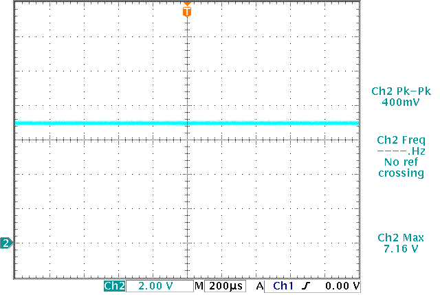
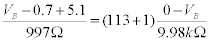
Figure 3. The DC offset for the transistor.
Figure 3 shows the DC offset for the transistor. This voltage is the same as VC. Notice that given VCC=15.1, the value of 7.16 V corresponds to a voltage drop across the resistor of 8.94 V. This is the offset we expected as we showed above.
Figure 4. Output for a 1kHz sinusoidal input. (Ch1 is the input and Ch 2 is the output. Notice that Ch2 has an offset of about 7V)
4) Now add an output coupling capacitor of 10 mF and observe the output. Measure the voltage gain. What does the output coupling capacitor do? Remember that the oscilloscope input acts as a 1 MW resistance to ground. Print out an oscilloscope image that clearly shows the input and the output.
Output coupling
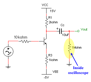
The gain of this circuit has been small because the 1k resistor on the emitter increases the voltage on the emitter (when current flows through it), which decreases the base-emitter voltage, which decreases the base current. We want the emitter resistor there as part of the biasing circuit (to stabilize the bias point), but we'd like to short it for the signal voltage. To do this we can add a bypass capacitor which effectively shorts the emitter to ground for AC signals, but doesn't effect the biasing.
|
For part 4.
Include your printout of the input and output. Explain any differences between the output in this step and that from the previous step.
Measure the gain of the circuit.
Calculate the gain of the circuit and compare to the measurement.
For DC analysis, we ignore the capacitor and assume the source is grounded. Then for the small signal model we have the following:
Small signal Parameters:
Gain:
Figure 5 shows the output of the circuit to a 2V peak to peak signal. The measured gain is -1.92V/V which compares really well with the calculated gain of -2V/V\.
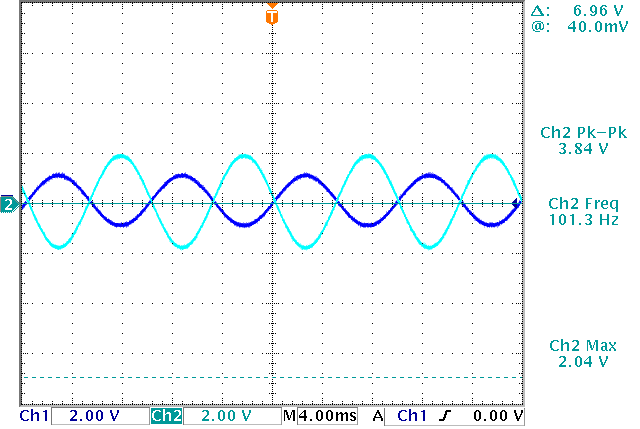
Figure 5. Output of the circuit to a 2V p-p input. (Ch1: input, Ch2: output)
5) Connect the circuit below (use a 330 mF capacitor for bypassing the emitter resistor) and measure the gain. Note the oscilloscope resistance is not shown. Explain qualitatively why the gain has increased. Also predict what the gain should be (assume the capacitors all behave as short circuits at 10 kHz). Adjust the input magnitude until the output is undistorted. Print out an oscilloscope image that clearly shows the input and the output.
Emitter bypassed
|
For part 5.
Include your printout of the input and output. Explain qualitatively why the gain is greater than that from the previous step.
Measure the gain of the circuit.
Calculate the gain of the circuit and compare to the measurement.
In the small signal model, the bypass capacitor acts like a short circuit. this increases the emitter current, which in turn increases both the base current and the collector current. The higher the collector current, the bigger the voltage drop across R1 becomes. Therefore, this circuit has a greater gain. The figure below shows the equivalent circuit.
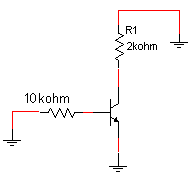
Figure 6 shows the emitter bypassed circuit output vs a small signal.
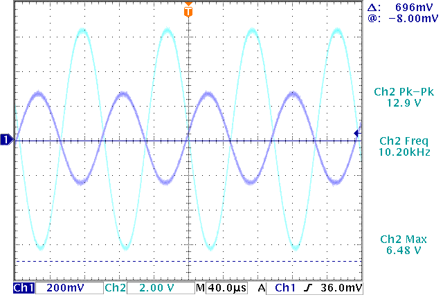
Figure 6. Emitter bypassed circuit output (Ch1: input, Ch2: output)
As seen in figure the measured gain is about -12.9/0.56=-23. Let's now find the calculated gain:
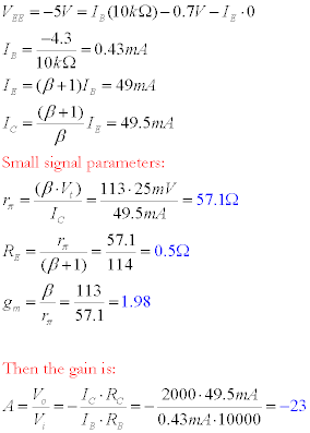
Both of our measured and calculated gain are -23. Assuming the capacitor has some impedance, we expected the measured gain to be slightly smaller (in magnitude) than -23 but surprisingly they match.
6) Adjust the input magnitude until both the top and the bottom of the signal are clipped. Identify which part of the distortion corresponds to saturation, and which part to cutoff. Print out an oscilloscope image that clearly shows the input and the output.
When you do the analysis of the gain of this circuit use superposition consider the capacitors to be short circuits for the AC signal.
|
6. Include your printout of the input and output. Identify saturation and cutoff.
When the transistor is in saturation the bottom part of the output starts to get flat. This is shown in Figure 7.The cutoff region makes the top part of the output go flat, and this is shown in Figure 8.
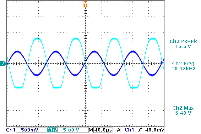
Figure 7. Operation in saturation (Ch1: input, Ch2: output)
Figure 8. Operation in cutoff (Ch1: input, Ch2: output)
A better voltage regulator.
Consider (but don't build) the circuit shown below, a modification of the zener-regulated circuit from last week, and sketch or print vi, vo and vx. Remember to us the 1/2 Watt 120 Ohm resistor. Use a 6.2V zener diode.
Zener regulator
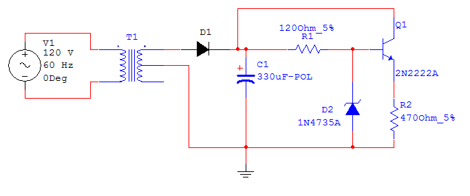
7) Explain why this circuit would work so much better than the simple zener regulator. Hint: Consider how much the current is varying in the zener diode.
|
7. Explain clearly why this circuit is better than the simple zener regulator from two weeks ago.
In the previous lab, we worked with a zener diode that was connected in parallel with the load. In that configuration, a small load resistance could potentially drain a huge current into the zener and push it beyond the knee point, causing the voltage drop to decrease significantly. With this circuit, the transistor keeps the current through the zener pretty much constant. The zener maintains the base voltage at an almost constant value, which causes and almost constant voltage at the emitter. Thus we end up with near constant currents through the emitter, base and collector. Slight voltage changes in the base are compensated for by the transistor and zener, therefore, all in all, we have a much stabler circuit.
8) Look up the LM324 datasheet. The LM324 is a quad op-amp that is used in situations that call for a single supply (e.g.., 0-9 V) instead of a split supply (e.g. +12 V). The output can go very close to the supply rails (recall that the 411 can only go within about 2 volts of the rail). Look up the datasheet to find the pinout. Use the voltage labeled Vx for the positive supply for the op amp.
Consider (but don't build) the circuit shown below. Predict the output voltage. Note that the 120 W resistor has been replaced by a 240 W resistor. Why is this possible?
Op-Amp regulator
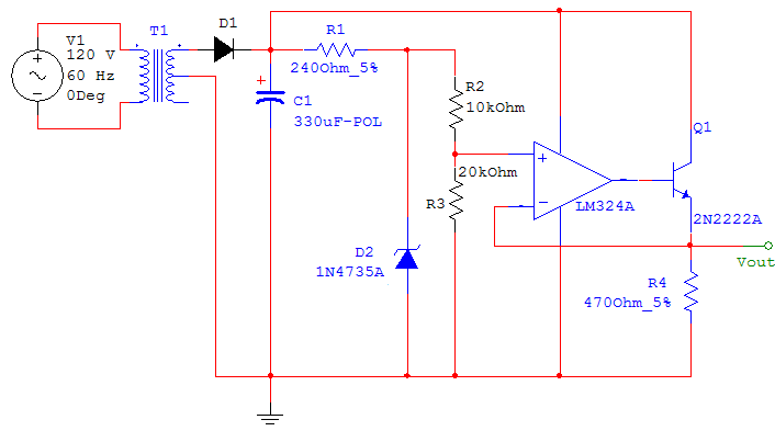
This circuit gives better regulation than the previous example (part 7). Why?
This circuit is roughly equivalent to the voltage regulator integrated circuit that you used in the previous lab.
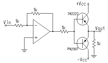
A Pumped-Up Op-Amp
A typical op-amp alone cannot output much current. Shown below is a circuit that is designed to remedy this by using two transistors to amplify the current coming out of the op-amp. This type of output is called a push-pull output stage because when the voltage from the op-amp is greater than 0.7 volts the NPN transistor pushes current into the load (the 1kW resistor at the output). When the op-amp output is less than -0.7 volts the PNP transistor pulls current from the load. Make sure you understand how this should work. Use a 2N2222 and PN2907 for the two transistors. Use Vcc=12 V.
Pumped-Up Op-Amp
|
For part 8
Predict the output voltage.
How does this circuit work?
Why is a 324 op amp required instead of a 411?
Let's look at the non-inverting input of the op-amp. R2 and R3 simply acts as a voltage divider to the voltage at the top of the zener. We have
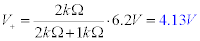
Since we have no current through the op-amp, the inverting and non-inverting terminals are at the same voltage. We can conclude then that Vout=V-=V+= 4.13V.
This circuit works even better than the transistor-zener voltage regulator from part 7 because the op-amp will try to maintain Vout at 4.13 and will supply any required current to the base to accomplish it no matter what the load resistence is.
This circuit is also superior to the circuit from part 7 in that, by choosing the values of R2 and R3 we can adjust the output voltage.
The reason for using the 324 op-amp instead of the 411 is because the 411 only allows its output terminal voltage to be within a fwe volts of the input voltages, whereas the output terminal voltage of the 324 can be moved all the way up to the voltage at the supply rails.
9) Build the circuit (use either an LF411 or an LM324) and attach the input to a 200 Hz sine wave. Look at the output of the op-amp, then the output of the push-pull stage. Note the distortion in Vout. This is called crossover distortion because it happens when the current crosses over from one transistor to the other. Print out an oscilloscope image that clearly shows the input and the output and the crossover distortion.
|
9. Include your printout of the input and output. Label and explain the crossover distortion.
The reason for crossover distortion is because the transistors are off when the output of the op-amp is between 0.5V and -0.5V. Not that they are still operating between 0.7 and 0.5 but in the linear region. Figure 9 shows the input voltage, the output of the op-amp and the overall output voltage. You can clearly observe the crossover distortion.
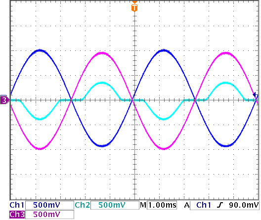
Figure 9. input and output voltages and the crossover distortion. (Ch1: Vin, Ch2:output voltage of the op-amp, Ch3:Vout)
10) Rearrange the circuit to eliminate the crossover distortion. (Hint: Where should the feedback come from to eliminate distortion in the output of the entire circuit? Currently the feedback comes from the output of the op-amp, so the op-amp does what it needs to do in order to ensure that its output is -10 times the input.) You only need to move one connection on the breadboard to get this to work. Come talk to me if you don't see the solution.
|
10. Include the schematic of your modified circuit, and the rational for your choice.
Here is the modified circuit:
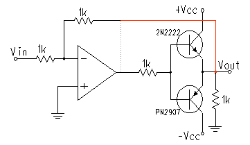
We chose to have the feedback come directly from the output voltage instead of the op-amp output becuse this way, the op-amp will try to make up for the crossover distortion by pushing current up and putting the transistors in the operating region. This circuit is now dependent on the slew rate of the op-amp because it will have to switch from low (but not zero) negative voltages to low (but not zero) positive voltages quickly in order to keep the output -1 times the input. This will be clearer in the following section.
11) With the distortion at the output stage gone, what does the output of the op amp look like? Print out an oscilloscope image that clearly shows the input and the op-amp output (not the circuit output).
Note that this circuit's frequency range is limited by the slew rate of the op-amp because the output must change instantaneously at the point where the current switches from the NPN transistor to the PNP. Increase the frequency of the input until you see the distortion in the output due to this effect. (It is also easier to see with smaller inputs, |Vin|<1 Volt).
|
11.Include your printout of the input and output of the op-amp. Explain why the output looks like it does.
Figure 10 shows the input and output of the revised op-amp.
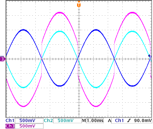
Figure 10. Output of the super-pumped-up op-amp. (Ch1: Vin, Ch2:Vout, Ch3:output voltage of the op-amp)
As we started to explain in the previous section, the op-amp will now have to swith its output very fast between negative and positive voltages to avoid crossover distortion. There are two things happening here:
1 - transistors don't operate under when |VBE|<0.7V.
2- the in order for the output voltage to be -Vin, the transistors have to remain on.
The only way this can happen is if the op-amp quickly switches it's output and feeds in the appropriate currents to keep the transistors on. and that's precisely what happens.
|