abstract.
For the first task, we built a parity checker which took as its inputs, a 4-bit binary number and one even parity bit. A circuit was designed in such a way that the number of 1's in the 4-bit binary number should be even when the parity bit is included. Another circuit was made to check whether or not a four-bit binary number was a prime number. For the second task, a digital circuit was designed and built to output the proper signaling sequence for a 4-way intersection.
description of task.
Task 1a: Parity Checker:
For the parity checker, a total of 5 binary values made up the inputs to the circuit. These inputs were a 4-bit binary number and one even parity bit. The 4-bit binary number is a binary representation of the numbers 0 through
15 in the decimal system. For example, the number "3" in decimal form would be "0011" in binary form. Each digit in the binary number is an input to the system and the fifth input is provided by the parity bit.
The function of this system was obtained by constructing a truth table from the inputs to the system, and then translating it into a Karnaugh map. From the Karnaugh map, an equation describing a possible circuit design for the system was extracted. The function that was obtained is f = A XOR B XOR C XOR D XOR P, where A, B, C, and D represent the four binary digits and P represents the parity bit. This equation was then implemented on a breadboard using XOR gates.
The output of this system is a single binary digit that is high when there is an uneven number of 1's in the five binary values of the input, and signals that the parity bit is in error. When there is an even number of 1's, the output is low or "0". The output of the function was displayed on one of the LEDs on the breadboard
Task 1b: Prime Number Checker
A circuit was designed to determine whether or not a number that was inputted in binary form was a prime number. Once again, each digit in the binary number is taken as a single input and passed through the circuit. To begin, a truth table was created and the inputs and output are placed in their corresponding spots in the Karnaugh map. The following equation was obtained from the Karnaugh map:  . Using this equation, a logic circuit was constructed on a breadboard. A series of on-off switches were used to represent and control the binary input to the circuit and the output was displayed on a LED on the breadboard. If the input was a prime number, then the output would be high and the LED would light. If the input was not a prime number, the output would be low and the LED would not light. . Using this equation, a logic circuit was constructed on a breadboard. A series of on-off switches were used to represent and control the binary input to the circuit and the output was displayed on a LED on the breadboard. If the input was a prime number, then the output would be high and the LED would light. If the input was not a prime number, the output would be low and the LED would not light.
Task 2: Traffic Light
For this task, a circuit was designed to output a traffic light signal pattern for a 4-way intersection. A binary counter was used and set up to provide a continuous and repeating signal, ranging from 0 to 15 in binary form. These binary values provided by the counter made up the four inputs to the system. In order to obtain the functions that describe the system, a truth table and Karnaugh map was made for all the different outputs of the system. An equation was obtained for North/South Red, East/West Red, North/South Yellow, and so on for all six outputs. This time, however, the output was considered active low, or when the value is 0, when looking at the truth tables and Karnaugh map. These equations and how they were obtained are detailed in the section that follows.
After obtaining the individual functions that defined the pattern of lighting for the different outputs, the circuit was then implemented on a breadboard. After the circuit was completed, the six outputs of the circuit were connected to the corresponding wires on a model traffic light to test whether the pattern generated by the circuit was correct.
design process.
In order to implement a function that would check for correctness in the parity of an input signal, we first created a truth table and an associated Karnaugh map for the circuit.
# |
BIN |
parity |
0 |
0000 |
0 |
1 |
0001 |
1 |
2 |
0010 |
1 |
3 |
0011 |
0 |
4 |
0100 |
1 |
5 |
0101 |
0 |
6 |
0110 |
0 |
7 |
0111 |
1 |
8 |
1000 |
1 |
9 |
1001 |
0 |
10 |
1010 |
0 |
11 |
1011 |
1 |
12 |
1100 |
0 |
13 |
1101 |
1 |
14 |
1110 |
1 |
15 |
1111 |
0 |
CD\AB |
00 |
01 |
11 |
10 |
00 |
0 |
1 |
0 |
1 |
01 |
1 |
0 |
1 |
0 |
11 |
0 |
1 |
0 |
1 |
10 |
1 |
0 |
1 |
0 |
f = A xor B xor C xor D
The same process was used when creating the function that would return a high output if the inputted number was prime.
# |
BIN |
PRIME? |
0 |
0000 |
0 |
1 |
0001 |
0 |
2 |
0010 |
1 |
3 |
0011 |
1 |
4 |
0100 |
0 |
5 |
0101 |
1 |
6 |
0110 |
0 |
7 |
0111 |
1 |
8 |
1000 |
0 |
9 |
1001 |
0 |
10 |
1010 |
0 |
11 |
1011 |
1 |
12 |
1100 |
0 |
13 |
1101 |
1 |
14 |
1110 |
0 |
15 |
1111 |
0 |
CD\AB |
00 |
01 |
11 |
10 |
00 |
0 |
0 |
0 |
0 |
01 |
0 |
1 |
0 |
1 |
11 |
1 |
1 |
1 |
0 |
10 |
1 |
0 |
0 |
0 |
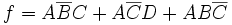
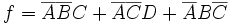
In order to implement the circuit for operating the traffic light, we had to create a separate truth table and Karnaugh map for each of the different lights. The maps for the pairs of same-color lights (as in, N/S red and E/W red) were very similar. Here are truth tables and Karnaugh maps for each. In this case, since the lights turn on when there is a low output, zeroes in the table represent when each light is on.
# |
Bin |
EW Green |
NS Green |
EW Yellow |
NS Yellow |
EW Red |
NS Red |
0 |
0000 |
1 |
1 |
1 |
1 |
0 |
0 |
1 |
0001 |
1 |
0 |
1 |
1 |
0 |
1 |
2 |
0010 |
1 |
0 |
1 |
1 |
0 |
1 |
3 |
0011 |
1 |
0 |
1 |
1 |
0 |
1 |
4 |
0100 |
1 |
0 |
1 |
1 |
0 |
1 |
5 |
0101 |
1 |
0 |
1 |
1 |
0 |
1 |
6 |
0110 |
1 |
1 |
1 |
0 |
0 |
1 |
7 |
0111 |
1 |
1 |
1 |
0 |
0 |
1 |
8 |
1000 |
1 |
1 |
1 |
1 |
0 |
0 |
9 |
1001 |
0 |
1 |
1 |
1 |
1 |
0 |
10 |
1010 |
0 |
1 |
1 |
1 |
1 |
0 |
11 |
1011 |
0 |
1 |
1 |
1 |
1 |
0 |
12 |
1100 |
0 |
1 |
1 |
1 |
1 |
0 |
13 |
1101 |
0 |
1 |
1 |
1 |
1 |
0 |
14 |
1110 |
1 |
1 |
0 |
1 |
1 |
0 |
15 |
1111 |
1 |
1 |
0 |
1 |
1 |
0 |
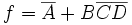
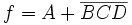
After looking at the Karnaugh maps for each of the functions, we decided that it would be easier to circle groups of zeroes and to use a NOT gate afterwards. Note that we used three main colors (green, red and yellow) and other colors are intersections of these main colors.
EW Green |
00 |
01 |
11 |
10 |
00 |
1 |
1 |
0 |
1 |
01 |
1 |
1 |
0 |
0 |
11 |
1 |
1 |
1 |
0 |
10 |
1 |
1 |
1 |
0 |
NS Green |
00 |
01 |
11 |
10 |
00 |
1 |
0 |
1 |
1 |
01 |
0 |
0 |
1 |
1 |
11 |
0 |
1 |
1 |
1 |
10 |
0 |
1 |
1 |
1 |
EW Yellow |
00 |
01 |
11 |
10 |
00 |
1 |
1 |
1 |
1 |
01 |
1 |
1 |
1 |
1 |
11 |
1 |
1 |
0 |
1 |
10 |
1 |
1 |
0 |
1 |
f = ABC
NS Yellow |
00 |
01 |
11 |
10 |
00 |
1 |
1 |
1 |
1 |
01 |
1 |
1 |
1 |
1 |
11 |
1 |
0 |
1 |
1 |
10 |
1 |
0 |
1 |
1 |

EW Red |
00 |
01 |
11 |
10 |
00 |
0 |
0 |
0 |
1 |
01 |
0 |
0 |
1 |
1 |
11 |
0 |
0 |
1 |
1 |
10 |
0 |
0 |
1 |
1 |
NS Red |
00 |
01 |
11 |
10 |
00 |
0 |
1 |
0 |
0 |
01 |
1 |
1 |
0 |
0 |
11 |
1 |
1 |
0 |
0 |
10 |
1 |
1 |
0 |
0 |
After finding each of these functions, the circuit could be designed and built to operate a traffic light with the given timing.
Final Circuit
For the first part (parity check) of task 1, we used XOR gates and simply connected the parity input E with the other four inputs as seen in fig1. We connected the output to an LED and expected the led to turn on when the parity was wrong. We implemented the circuit using 74HC86N, a quad 2-input XOR gate.
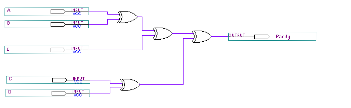
fig 1: parity check circuit
The second part of task 1 was about designing a circuit that told us whether the input was prime or not (namely, the output of the circuit was high when the input was 2, 3, 5, 7, 11 or 13 and low otherwise). We implemented the circuit seen in fig2 using a NOR gate instead of the OR gate and inverting the output.
In fig2, we labelled the AND gates abC, aBD, BcD and bCD; a small letter means that the input was inverted (ie. abC is A' B' C).
We implemented the circuit using a HEX inverter (7404), two TRIPLE 3-input AND gates (7411) and a DUAL 4-input NOR gate (7425).
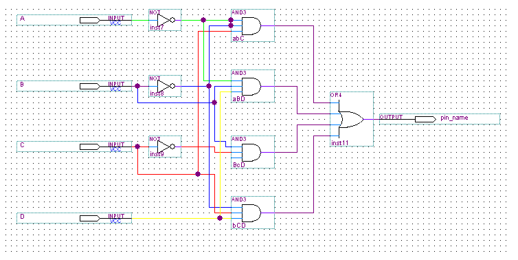
fig 2 : logic diagram for the prime numbers circuit.
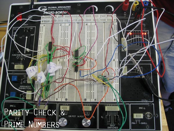
pic 1: the parity check and prime number circuits seen together
|
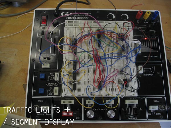
pic2: traffic lights and the 7-segment display circuits seen together
|
For task 2, we used the circuit illustrated in fig 3. For the OR gates we used NOR gates, and since the traffic lights worked with low input, we didn't need to invert them in the actual circuit. Similarly, the inverted AND gates, seen at the top of fig 3, weren't inverted. For the inputs we used a binary counter (74191) so that we could simulate the traffic lights better.

fig 3 : logic diagram for the traffic lights circuit
As an extension to our lab, we chose to do the 7-segment display. We simply connected the outputs from the binary counter to the Binary-to-7-segment-display converter. Then the outputs from the converter were used as inputs to the display (we had to
Testing the Circuits
All of our circuits worked well. In order to test the first two circuits, we connected the inputs to the first four Logic Indicators found on the right side of the breadboard. We connected the parity check to the very last indicator, and the prime number indicator was placed next to it. We used the DIP SWITCH to test every possible input. (Since we could see the input and the resulting outputs together on the logic indicators, it was easier to test the circuit.)
For the second task (traffic lights), we again connected the inputs to the first four Indicators. Then, we tested each of the outputs (N/S red, N/S yellow and so on) using the last indicator. Again, it was very helpful to connect the inputs to the indicators. Once we tested the traffic lights circuit on the breadboard, we implemented the 7-segment display, using the same binary counter. We encountered some problems testing the 7-segment display; the f LED didn't work right, therefore we disconnected the f LED from the binary counter and implemented a special circuit for it. We didn't have any problems with the other segments. Finally, we used the real traffic lights together with the 7-segment display to test both circuits and everything worked right.
What We Learned
Through the course of this experiment, we learned about the various logic gates and chips used in circuit design and the different operations they perform or functions they serve. Furthermore, we were able to obtain a good grasp on the steps involved in designing and creating a circuit. We are now able to go from a truth table to a Karnaugh map and then to a logic diagram. With the logic diagram written out, we are able to construct a circuit that performs the operations we seek. In addition, we now have a good understanding of the way these logic circuits are implemented in various devices around us. |